


N-Channel vs P-Channel MOSFETs in BMS: Which One Belongs Where?
2026-03-30
In Battery Management System design, choosing between N-Channel and P-Channel MOSFETs is not just a specification decision — it is a circuit topology decision. Use the wrong type in the wrong position and you will face inefficient switching, unreliable gate drive, or premature device failure.
This article walks through the major circuit positions inside a BMS and explains exactly which MOSFET type belongs where, and why.
Understanding the Core Difference
Before diving into circuit positions, it helps to understand the fundamental difference between the two types at a circuit level.
An N-Channel MOSFET turns on when the gate voltage is higher than the source voltage — typically needing Vgs of +4V to +10V. Because it uses electrons as charge carriers, it achieves lower Rds(on) per unit die area than a P-Channel device. This makes it the preferred choice for power-critical paths.
A P-Channel MOSFET turns on when the gate voltage is lower than the source voltage — typically needing Vgs of -4V to -10V. It uses holes as charge carriers, resulting in slightly higher Rds(on), but it offers a major circuit advantage: in a high-side position where the source sits at battery voltage, a P-Channel can be switched on by simply pulling the gate low — no bootstrap or charge pump required.
The diagram below shows the key difference in gate drive logic:

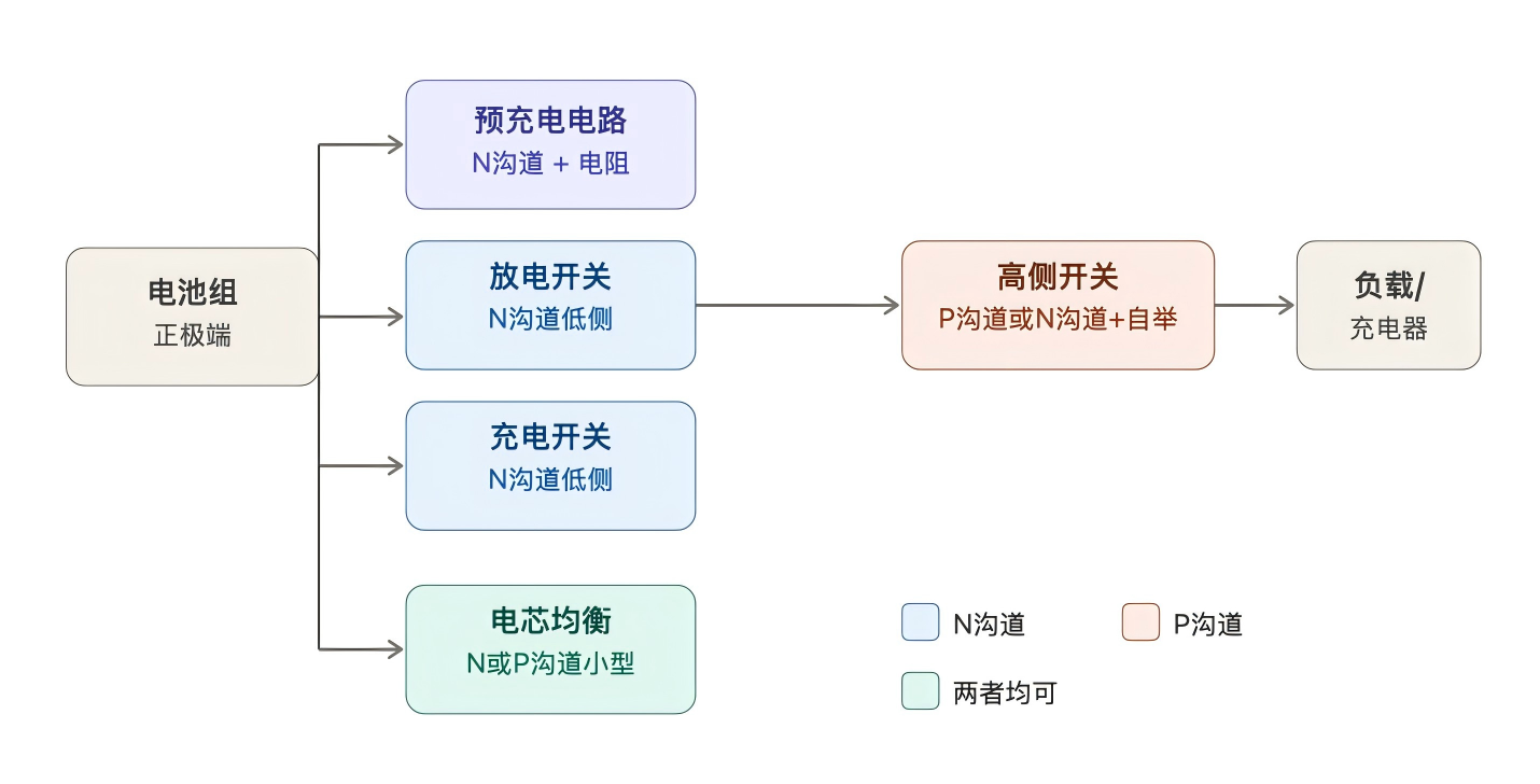
The BMS Circuit Positions
A typical lithium-ion BMS has several distinct switching positions — each with different requirements. The main power path uses back-to-back N-Channel MOSFETs for both charge and discharge control. The pre-charge circuit protects the main switches from inrush current. Cell balancing uses small MOSFETs per cell. High-side positions may use either type depending on gate drive availability.
The diagram below shows the full BMS topology at a glance:
Main Discharge and Charge Switches
These are the two most critical positions in any BMS. Both carry the full battery current — every ampere that flows in or out passes through these switches. N-Channel MOSFETs are the universal standard here.
The reason is straightforward: in a low-side configuration, the source pin is connected to ground. This means the gate only needs a voltage of +5V to +10V above ground to switch the device on — which any standard gate driver or microcontroller can provide directly without additional circuitry.
The most common arrangement is a back-to-back configuration — two N-Channel MOSFETs placed in series with their sources connected together. This allows the BMS IC to independently open or close the charge path and the discharge path. When both are closed, current flows freely. When the charge switch opens, the battery cannot receive current from a charger. When the discharge switch opens, the battery cannot supply current to the load.
For this position, the key parameters are low Rds(on) to minimize heat and conduction loss, high continuous current rating, strong avalanche ruggedness for protection against inductive load spikes, and a compact thermally efficient package.
GOFORD recommendation: For standard lithium-ion BMS main switching, the GT043N15TLAand GT020N10TLAare strong candidates for high-current demanding designs. For more compact board layouts, the GT105N10D5delivers excellent Rds(on) in a small footprint. All GOFORD N-Channel parts are 100% avalanche tested for reliable surge protection.
Part Number | Package | Vds(V) | Id(A) | Rds(on)mΩ(typ) @Vgs=10V | Rds(on)mΩ(typ) @Vgs=4.5V | Qg(nC) | Ciss(pF) |
DFN5*6-8L | 100 | 63 | 8.5 | 38 | 1600 | ||
TOLL-8L | 100 | 313 | 1.65 | 160 | 10600 | ||
TOLL-8L | 150 | 202 | 3.8 | 75.3 | 5007 |
Pre-Charge Circuit
When a BMS first connects to a load such as a motor inverter or DC-DC converter, the load's input capacitance is initially uncharged. Connecting a fully charged battery to an empty capacitor creates a massive inrush current spike — capable of destroying the main MOSFETs, blowing fuses, or damaging the load.
The pre-charge circuit solves this by inserting a series resistor in parallel with the main discharge switch. The pre-charge MOSFET closes first — allowing current to flow through the resistor and charge the load capacitance gradually. Once the load voltage reaches close to battery voltage, the main discharge switch closes and the pre-charge switch opens.
N-Channel MOSFETs are used here. The electrical requirements are different from the main path — current is limited by the resistor, so high Rds(on) is less critical. What matters most is wide Safe Operating Area (SOA), the ability to handle repetitive switching cycles reliably, and sufficient pulse current capability.
GOFORD recommendation: For pre-charge applications in 100V BMS systems, the GT048N10TA offers a good balance of current capability and controlled switching. For space-constrained designs, the GT105N10D5 fits well on compact BMS PCBs.
Part Number | Package | Vds(V) | Id(A) | Rds(on)mΩ(typ) @Vgs=10V | Rds(on)mΩ(typ) @Vgs=4.5V | Qg(nC) | Ciss(pF) |
DFN5*6-8L | 100 | 63 | 8.5 | 38 | 1600 | ||
TO-220 | 100 | 110 | 4.4 | 5.2 | 68 | 3200 |
Cell Balancing
Individual cells in a battery pack age at different rates and develop slightly different charge levels over time. Left unmanaged, the weakest cell limits the entire pack capacity and accelerates degradation. Cell balancing corrects this by redistributing charge between cells.
In passive balancing, a resistor is switched across any cell that is above the target voltage, bleeding off excess charge as heat. Small N-Channel or P-Channel MOSFETs work here — the voltage per cell is low (3–4.2V for lithium-ion) and current is small. Low Vgs(th) is the priority so the MOSFET switches reliably from a low-voltage BMS IC output.
In active balancing, energy is transferred between cells using inductors or capacitors. N-Channel MOSFETs are strongly preferred here due to their lower gate charge, faster switching speed, and lower Rds(on).
GOFORD recommendation: For cell balancing switches in compact BMS designs, the G1002 and GT1K2N10I are ideal — small footprint, low leakage, suitable for per-cell switching logic. For P-Channel passive balancing where negative gate drive is available, the 2301A and G500P03LL are compact options.
| Part Number | Package | Vds(V) | Id(A) | Rds(on)mΩ(typ) @Vgs=10V | Rds(on)mΩ(typ) @Vgs=4.5V | Qg(nC) | Ciss(pF) |
| G500P03LL | SOT-23-6L | -30 | -4.6 | 40 | 70 | 13 | 680 |
| 2301A | SOT-23 | -20 | -3 | 42 | 8.5 | 640 | |
| G1002 | SOT-23 | 100 | 2 | 195 | 205 | 22 | 450 |
| GT1K2N10I | SOT-23 | 100 | 3.3 | 91 | 113 | 4.2 | 145 |
High-Side Switching
When the design requires a switch between the battery positive terminal and the load — a high-side position — gate drive becomes more complex for N-Channel devices. The source pin floats at close to battery voltage, so the gate must be driven to battery voltage plus 5–10V. This requires a bootstrap capacitor circuit or a dedicated charge pump, adding cost and circuit complexity.
P-Channel MOSFETs offer an elegant alternative for high-side switching. Since they turn on when the gate is pulled low relative to the source, a simple logic-level pull-down referenced to battery positive is sufficient. No bootstrap, no charge pump. The trade-off is higher Rds(on) — typically 2–3× higher than an equivalent N-Channel die — and lower maximum current.
For applications where circuit simplicity matters more than peak efficiency — such as active clamp circuits, H-bridge high-side switches in lighting, and moderate-power DC-DC topologies — P-Channel MOSFETs are an excellent fit. The simplified gate drive reduces BOM cost and board complexity, making them a practical choice for these scenarios.
For high-current EV and energy storage main paths, N-Channel with bootstrap driver is still preferred for efficiency.
GOFORD recommendation: For P-Channel high-side switching in BMS and power management applications, GOFORD offers a comprehensive lineup. The GT2K0P20M) and GT2K0P20K are strong choices for high-voltage high-side applications requiring automotive-grade reliability. For lower voltage designs around 100V, the GT400P10K and GT750P10D5offer compact high-side solutions with excellent Rds(on). For the most space-constrained 150V designs, the GT880P15D5 and GT880P15K deliver ultra-low Rds(on) in multiple package options.
| Part Number | Package | Vds(V) | Id(A) | Rds(on)mΩ(typ) @Vgs=10V | Rds(on)mΩ(typ) @Vgs=4.5V | Qg(nC) | Ciss(pF) |
| GT2K0P20M | TO-263 | -200 | -19 | 166 | 179 | 57 | 3400 |
| GT2K0P20K | TO-252 | -200 | -18 | 180 | 190 | 70 | 3400 |
| GT880P15D5 | DFN5*6-8L | -150 | -30 | 82 | 94 | 46 | 3350 |
| GT880P15K | TO-252 | -150 | -30 | 80 | 90 | 46 | 3350 |
| GT400P10K | TO-252 | -100 | -35 | 29 | 34 | 41 | 3128 |
| GT750P10D5 | DFN5*6-8L | -100 | -24 | 50 | 62 | 40 | 1930 |
Quick Reference Table
The following summarizes the complete MOSFET placement logic for a BMS:

Conclusion
The choice between N-Channel and P-Channel in BMS design is driven by circuit topology, not personal preference. N-Channel MOSFETs dominate the power-critical positions — main switching, pre-charge, and active balancing — because of their lower Rds(on) and simpler gate drive in low-side configurations. P-Channel MOSFETs earn their place in high-side applications where eliminating the bootstrap circuit simplifies the design.
Understanding this topology logic before selecting a part number leads to better designs, lower losses, and more reliable battery systems.
GOFORD Semiconductor offers a comprehensive range of both N-Channel and P-Channel MOSFETs optimized for every BMS position — from ultra-compact SOT-23 cell balancing devices to high-current TOLL-8L main switching parts and AEC-Q101 qualified automotive-grade solutions. All devices are 100% avalanche tested for reliability in demanding battery applications.
 Latest news
-
2026-03-30
BMS Safety Starts with the Right MOSFET Selection
-
2026-03-30
N-Channel vs P-Channel MOSFETs in BMS: Which One Belongs Where?
-
2026-03-05
MOSFET Thermal Design and Reliability in BMS Systems
-
2025-12-25
Goford 150V P-MOSFETs: Ultra-Low RDS(on) for High-Power Apps
-
2025-12-25
Ultra-Low Resistance MOSFETs for Advanced Power Systems